The research of Sun group is focused on the photophysics of novel semiconductors. They include metal oxides and nanomaterials (e.g., nanosheets,
nanorods, and quantum dots). The novel properties of the nanomaterials originate at the quantum confinement at the nanometer scale. For instance,
tunable and pure-color light emission can be achieved by simply changing the size of quantum dots, which is the science behind the new quantum-dot
LED (QLED) TVs made by Samsung. Our current research on nanomaterials aims at the anisotropic nanocrystals with emphasis on nanosheets. The anisotropic
confinement of the exciton in nanosheets results in new properties different from isotropic quantum dots, such as slower Auger processes, giant
oscillator strength transition, high photoluminescence quantum yield, and low-threshold lasing. These new photophysics properties are studied using
time-resolved laser spectroscopy and other material characterization methods including electron microscopy, XRD, FTIR, and Raman spectroscopy.
Our research on metal oxides aims at the color centers in ultra-wide-bandgap semiconductors. The large-band-gap metal oxide can host and protect
the quantum states of the defect states (color centers) that can be utilized for quantum information processing. We are developing methods to create
these color centers and study their quantum properties using techniques including pulsed electron paramagnetic resonance, Hanbury−Brown and Twiss setup,
and Hong–Ou–Mandel quantum interference.
The students in Sun group will learn and master many experimental techniques for nanomaterial research, including electron microscopy
(such as TEM and SEM), UV-Vis-IR spectroscopy, laser technology, synthesis of nanostructured materials, optoelectronic device fabrication
and testing, and quantum optics. In the process of research, they will participate in planning future research and setting up the experimental apparatus.
In such a way, they will gain significant critical-thinking and problem-solving skills.
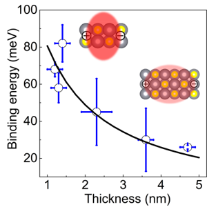
Two-dimensional colloidal PbS nanosheets exhibit more than one order of magnitude larger exciton binding energy than their bulk counterpart,
making it possible to generate stable excitons at room temperature. It is experimentally revealed that the binding energy of the exciton increases
from 26 to 68 meV as the thickness of the PbS nanosheet decreases from 4.7 to 1.2 nm. The dielectric confinement of the exciton plays a critical role
in the binding-energy enhancement. The large binding energy results in a fast thickness-dependent exciton radiative recombination rate,
confirmed experimentally.
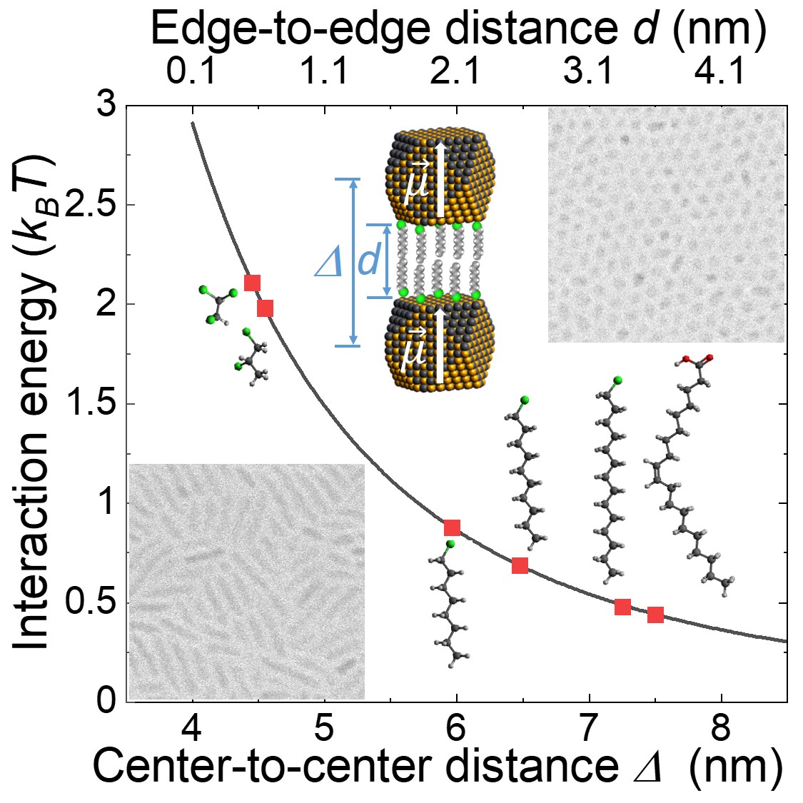
The electrical dipolar interaction between the quantum dots can be used to control the growth of colloidal PbSe nanorods.
The interaction energy can be tuned from a fraction to a multiple of the thermal energy. Consequently, the one-dimensional oriented attachment can be switched
on or off, as is the growth of nanorods.
J. Phys. Chem. Lett. 2021, 12, 1, 232–237 (2018)
Colloidal lead sulfide (PbS) nanoribbons are synthesized using organometallic precursors with chloroalkane co-solvents. The few-atom-thick nanoribbons have a
typical width 20 nm and a length more than 50 nm. Different from a nanosheet where the quantum confinement energy is mainly determined by the thickness, the
narrow width of the nanoribbon has an additional contribution to the increase of energy gap. In contrast to nanosheets, the nanoribbons are much brighter.
At room temperatures, well-passivated nanoribbons have achieved more than 30% photoluminescence quantum yield in the infrared spectrum, competing with the
well-developed colloidal lead chalcogenide quantum dots of the similar energy gap.
Chem. Mater. DOI: 10.1021/acs.chemmater.8b00467 (2018)
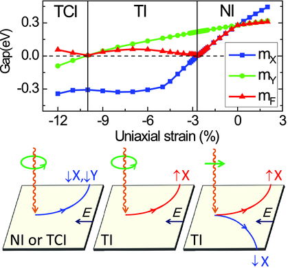
A PbS monolayer is demonstrated to be a novel platform for topological, valleytronic, and optical phenomena. Compressive strain
can turn the trivial monolayer into a topological insulator. Optical pumping can facilitate charge, spin, and valley Hall
effects tunable by external strain and light ellipticity. Similar results apply to other IV–VI semiconductors.
Adv. Mater. 29, 1604788 (2017)
In the synthesis of colloidal PbS nanosheets, acetic acid – either injected externally or produced during the reaction – has a
significant effect on the growth of the nanosheets. When the acetic acid to lead molar ratio is above 1:8, no nanosheets are
observed in the product. By replacing lead acetate with lead oxide to prepare the lead precursor for the reaction, the effect
of acetic acid is avoided, resulting in a robust synthesis with nearly 100% success rate. In the new synthesis, the purity of
trioctylphosphine (the co‐solvent for sulfur precursor) has no significant effect on the formation of nanosheets. Thickness
tunability is achieved in the acetate‐free synthesis by tuning the reaction temperature.
Phys. Status Solidi RRL 10, 838 (2016)
Catalyst‐free, one‐pot synthesis of colloidal PbSe nanorods is demonstrated. The co‐solvent chloroalkanes play a critical role
in driving a one‐dimensional growth of PbSe nanorods. The formation of the nanorod is likely governed by the anisotropic growth
of the crystal due to the different reactivity of the facets. The photoluminescence quantum yield of the nanorods is above 25%,
indicating well‐passivated surfaces.
Phys. Status Solidi RRL 10, 833 (2016)
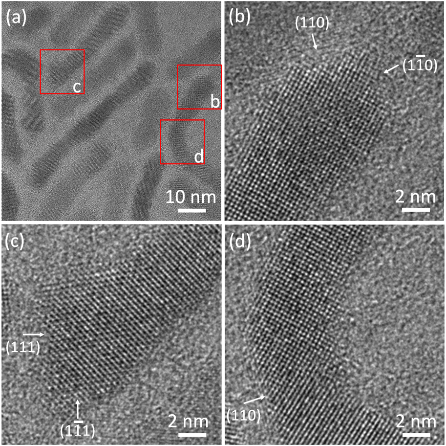
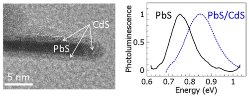
Emissive PbS/CdS core/shell nanosheets are synthesized using a cation-exchange method. A significant blue-shift of the photoluminescence is observed,
indicating a stronger quantum confinement in the PbS core as its thickness is reduced. High resolution transmission-electron-microscopy images of
the cross sections of the core/shell nanosheets show atomically sharp interfaces between PbS and CdS. Accurate analysis of the thickness of each layer
reveals the relationship between the energy gap and the thickness in the extremely one-dimensionally confined nanostructure. Photoluminescence lifetime
of the core/shell nanosheets is significantly longer than the core-only nanosheets, indicating better surface passivation.
Chem. Mater. 28, 5342 (2016)
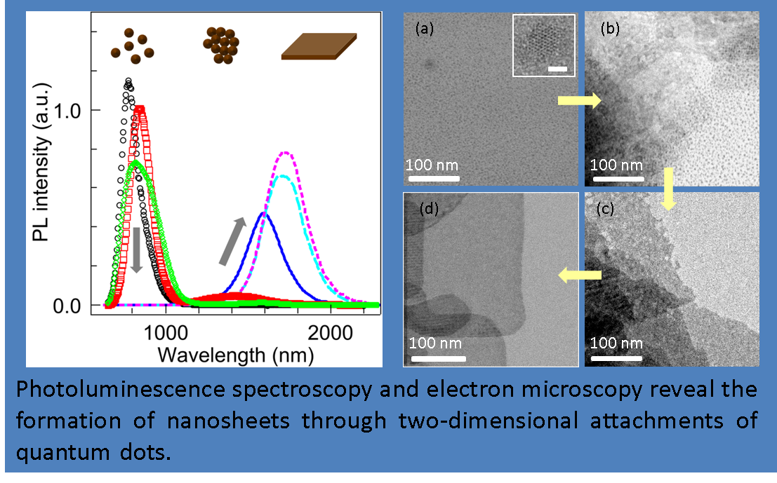
Dual photoluminescence peaks observed during the synthesis of colloidal PbS nanosheets reveal their growth mechanism – two-dimensional attachments of the quantum dots.
Well-grown nanosheets show the photoluminescence linewidth of 95 meV at room temperature. Aged nanosheets in toluene have enhanced photoluminescence with intensity
improved by an order of magnitude.
Phys. Chem. Chem. Phys. 17, 23303 (2015)
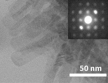
Single-crystal PbS nanosheets with thickness from 1.2 nm to 4.6 nm are synthesized using a thickness-controlled method. Their
thickness-dependent infrared photoluminescence are reported for the first time. The dependence of the energy gap on the thickness
(L) is found to follow a 1/L law, confirmed by density-functional-theory calculations.
Chem. Mater., 2014, 26 (19), pp 5433–5436
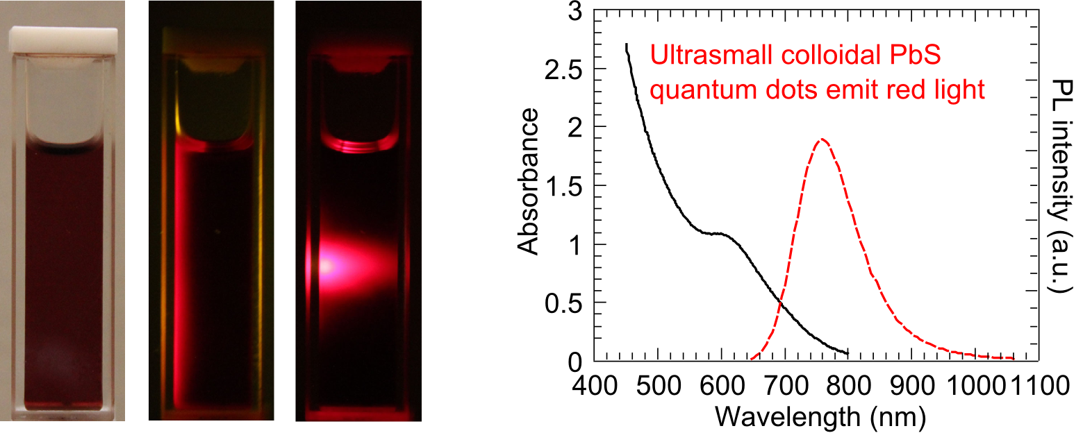
Ultrasmall colloidal lead sulfide quantum dots can increase the open circuit voltages of quantum-dot-based solar cells because of their large energy gap. Their small
size and visible or near infrared light-emitting property make them attractive to the applications of biological fluorescence labeling. Through a modified organometallic
route, we can synthesize lead sulfide quantum dots as small as 1.6 nm in diameter. The low reaction temperature and the addition of a chloroalkane cosolvent decrease the
reaction rate, making it possible to obtain the ultrasmall quantum dots. This work has been published in
Materials Chemistry and Physics .


Earlier research work
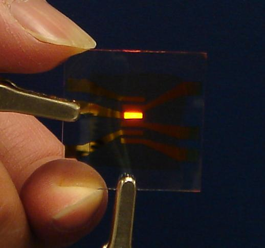
Infrared light-emitting diodes (LEDs) find application in night vision, optical-fiber
communications and free-space optical communications (such as the remote control units
of many commercial products including televisions and DVD players). Traditional LEDs
are fabricated using planar epitaxial technology – a manufacturing process used in
semiconductor industry, which needs a high-temperature and high-vacuum environment.
In contrast, LEDs based on colloidal nanocrystals can be fabricated at low temperature
and by solution chemistry, which can dramatically reduce the fabrication cost. Moreover,
the emission wavelength from the LEDs based on nanocrystals can be tuned easily by only
changing the size of the nanocrystals, which benefits from quantum confinement – a
fundamental phenomenon governed by quantum mechanics. That is to say, smaller nanocrystals
emit shorter-wavelength light while larger nanocrystals emit longer-wavelength light.
In our research, we can tune the emission wavelength from 800 nm to 1800 nm by changing
the size of the lead sulfide (PbS) nanocrystals from 2.7 nm to 6.5 nm. By optimizing the
balance of charge-carrier transport and recombination in the nanocrystal thin film, we
have achieved dramatic improvements in the performance of infrared emitters based on
colloidal semiconductor nanocrystals. In particular, the brightness is an order of
magnitude higher than in previous nanocrystal devices. These solution-processed devices
can compete with the performance of state-of-the-art infrared LEDs fabricated by planar
epitaxial technology.
This work was featured in a recent issue of
Nature Nanotechnology, the leading journal worldwide
in the area of nanotechnology. Figures below show the strucutre of a colloical
quantum-dots-based LED (left) and the tunability of the LEDs (right).

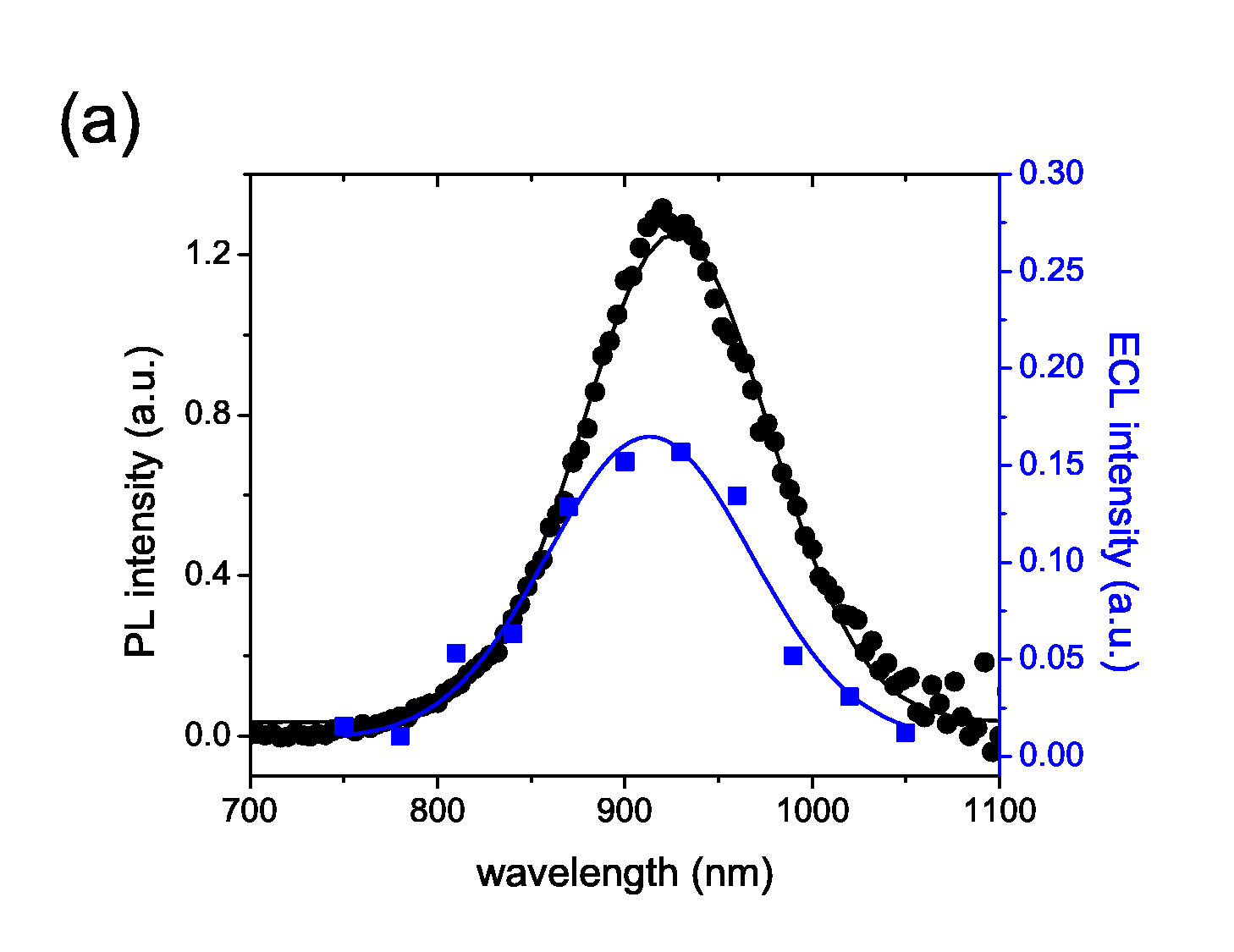
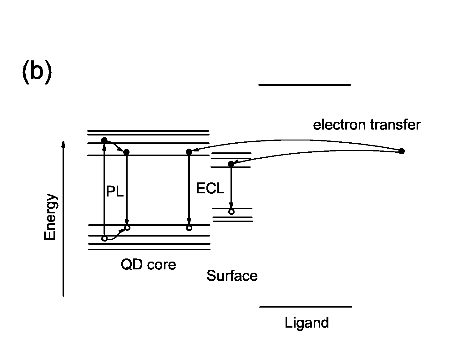
We are the first group who observed electrogenerated chemiluminescence (ECL) from PbS quantum dots
(QDs). Different ECL intensities are observed for different ligands used to passivate the QDs,
which indicates that ECL is sensitive to surface chemistry, with the potential to serve as a
powerful probe of surface states and charge transfer dynamics in QDs. In particular, passivation
of the QD surfaces with trioctylphosphine (TOP) increases ECL intensity by 3 orders of magnitude
when compared to passivation with oleic acid (OA) alone. The observed overlap of the ECL and
photoluminescence spectra suggests a significant reduction of deep surface trap states from the
QDs passivated with TOP. [
Nano Lett. 9, 789 (2009)]
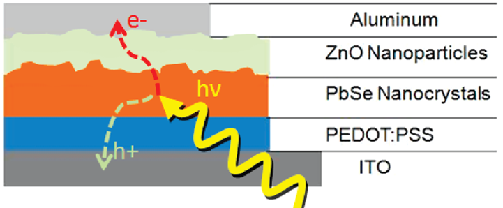
Lead-salt (PbS, PbSe etc.) quantum dots are used for fabricating solar cells. The power conversion efficiency of our excitonic
solar cell ranks among the highest performing quantum-dot-based solar cells reported to date.
[
Nano Lett. 9, 3749 (2009)]
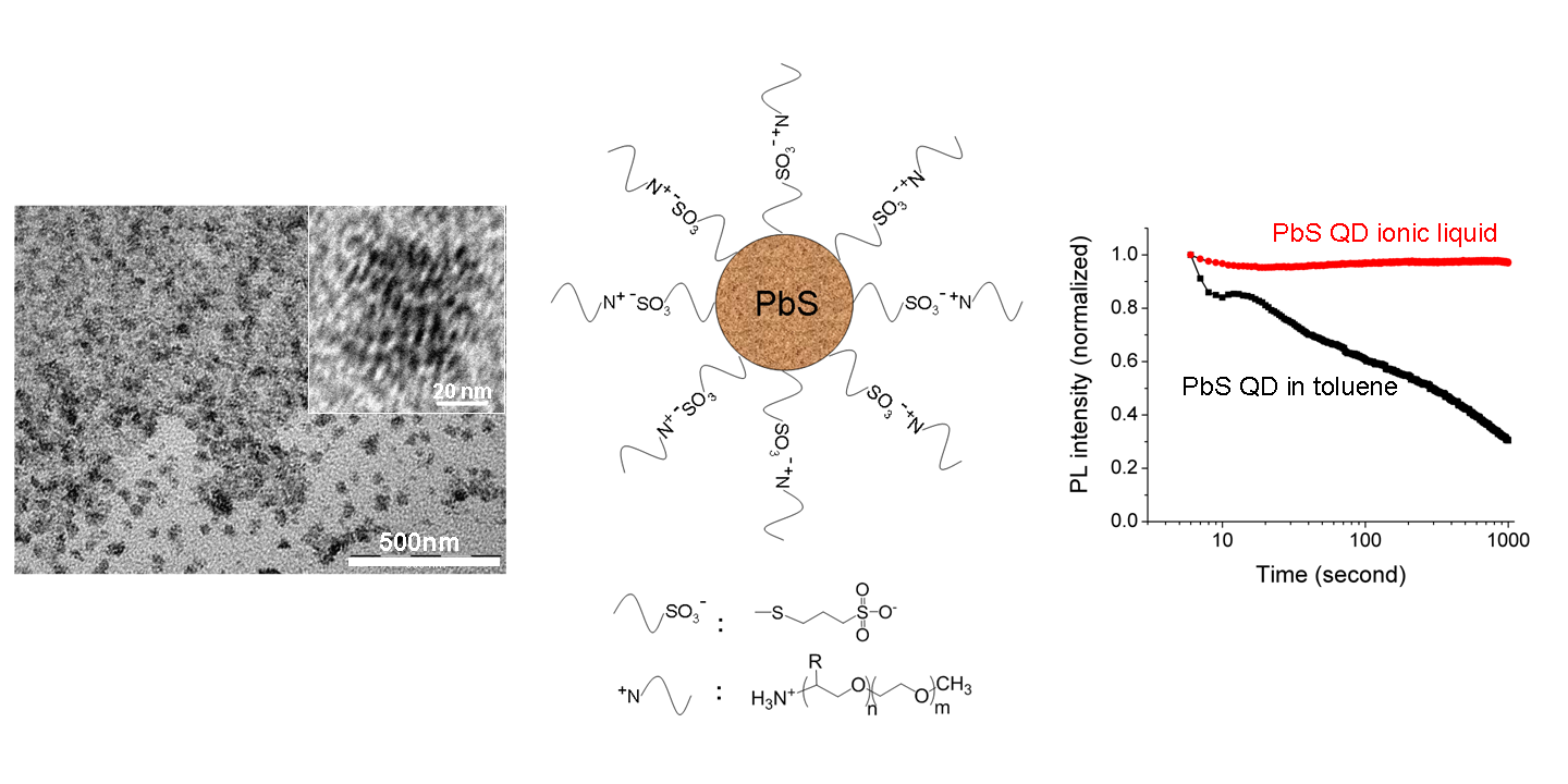
PbS quantum dots (QDs) are functionalized using ionic liquids with thiol moieties as capping ligands. The resulting
amphiphilic QD ionic liquids exhibit fluid-like behavior at room temperature even in the absence of solvents.
The photo-stability of the QDs is dramatically improved compared to oleic acid capped QDs dispersed in toluene (see picture).
[
Mater. Res. Soc. Symp. Proc. Vol 1114E, 1114-G08-27 (2009),
ACS 238th National Meeting (2009),
Small 6, 638 (2010)]
ITMCs (e.g. [Ru(bpy)
3(PF
6)
2] are used as active matrials for light emitting in OLEDs. By changing the centeral metal atom and the organic ligands, the HOMO and LUMO of the complex can be tuned, so the tunable electroluminescent wavelength can be obtained. Using gold and ITO electrodes, a simple air-stable iTMC OLED can be made.
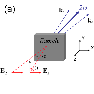
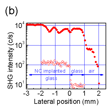
Optical second-harmonic generation (SHG) is used as a noninvasive probe of the interfaces of Si
nanocrystals (NCs) embedded uniformly in an SiO
2 matrix. Measurements of the generated SH mode verify that
the second-harmonic polarization has a nonlocal dipole form proportional to (
E·∇)
E that depends
on inhomogeneities in the incident field
E, as proposed in recent models based on a locally noncentrosymmetric
dipolar response averaged over the spherical NC interfaces. A two-beam SHG geometry is found to enhance this polarization
greatly compared to single-beam SHG, yielding strong signals useful for scanning, spectroscopy, and real-time monitoring.
This configuration provides a general strategy for enhancing the second-order nonlinear response of centrosymmetric samples,
as demonstrated here for both Si nanocomposites and their glass substrates.
[
Phys. Rev. Lett. 94, 047401 (2005),
Opt. Lett. 30, 2287 (2005),
Optics & Photonic News (2005)]